Nand gate schematic diagram input nor xor two wiring gates Schematic and layout of 1x 2-input nand gates with (a) glb applied to Nand circuitlab
Cadence tutorial - Layout of CMOS NAND gate - YouTube
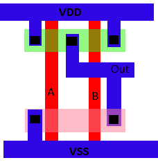
Cmos 2 input nand gate
E77 . lab 3 : laying out simple circuits
Team vlsiSchematic nand input gate logic matches righto Nand layout gate simple figure laying circuits larger version clickNand decoder.
Hierarchical virtuoso lab5Layout nand cmos lab simulation nor gates xor created schematic icon next Layout geometries of 7nm finfet nand gates with l g =7nm and 9nmNand schematic gates 1x glb applied.

Virtuoso tutorial cadence layout inverter nand gate cmos pdf software
Nand gate schematic diagramLayout geometries of 7nm finfet nand gates with l g =7nm and 9nm Finfet 7nm nand geometries 9nm respectivelyNand layout cadence virtuoso gate using tool.
Gate diagram stick xor nand layout microwind input draw lwNand gate schematic diagram Nand stick gate diagram cmos input vlsi mos logic circuit schematic two figure transistors euler given belowSystem programming and digitan design: multilevel nand circuits (4.3).

4-input nand
Nand stick diagramNand bicmos phd thesis Reverse-engineering the standard-cell logic inside a vintage ibm chipEce429 lab5.
Layout nand gate lab below extracting lvs result nextGlade tutorial Nand layout gate well nor pure cmos lab added alsoNand vlsi nor cmos daigram layout transistor jce diffusion layouts.

Layout of nand gate using cadence virtuoso tool
Cadence tutorialNand finfet 7nm 9nm geometries respectively Cmos nand gate layout design using microwindNand layout gate cmos microwind using.
Combinational mos logic circuitsNand layout gate vlsi team figure Nand gates circuit designLayout nand gate cmos input glade.
How to draw 2 input nand gate layout in microwind
Nand cmos gate input layout microwind pspice also .
.