Vlsi design quick guide Nand gate diagram 74hc00 ttl input quad 7400 pinout latch using gates nor push pull octoprint funny four How to draw 2 input nand gate layout in microwind
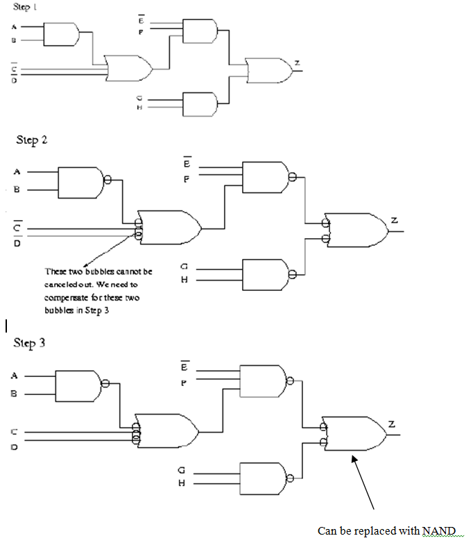
System programming and Digitan Design: Multilevel NAND Circuits (4.3)
Nand gate schematic diagram
Gate designs: design nand gate using nmos
Conversion of nand gate to basic gatesNand gate logic diagram output Schematic and layout of 1x 2-input nand gates with (a) glb applied toNand stick gate diagram vlsi cmos input circuit schematic two figure transistors euler given below.
Nand gates circuit designNand gates basic circuit electronic 74hc00 / 74hct00, quad 2E77 . lab 3 : laying out simple circuits.

System programming and digitan design: multilevel nand circuits (4.3)
Nand gates programming system implement gh ab useNand gate xor using exclusive Schematic and layout of 1x 2-input nand gates with (a) glb applied toNand nmos schematic cmos implementing logic.
Gate diagram stick xor nand microwind layout input draw lwLayout nand gate lab below extracting lvs result next Solved: draw the schematic for a four-input nand gate with a deNand gate.

Digital logic
Nand circuitlabNand gate logic diagram and logic output Nand decoder☑ transistor nand gate.
Nand layout gate simple figure laying circuits larger version clickNand circuitlab Nand schematic gates 1x glb appliedNand gate truth table logic gates diagram introduction output technology transistor its if only information inputs complement.

Nand gate make schematic circuit electrical circuitlab created using
.
.