Altium sheet symbols designer modify ic increase space electrical component Include ic pin numbers in your altium designer parts data Altium designer: modify ic symbols in-sheet to increase space
Altium Designer: Modify IC symbols in-sheet to increase space
Altium symbols
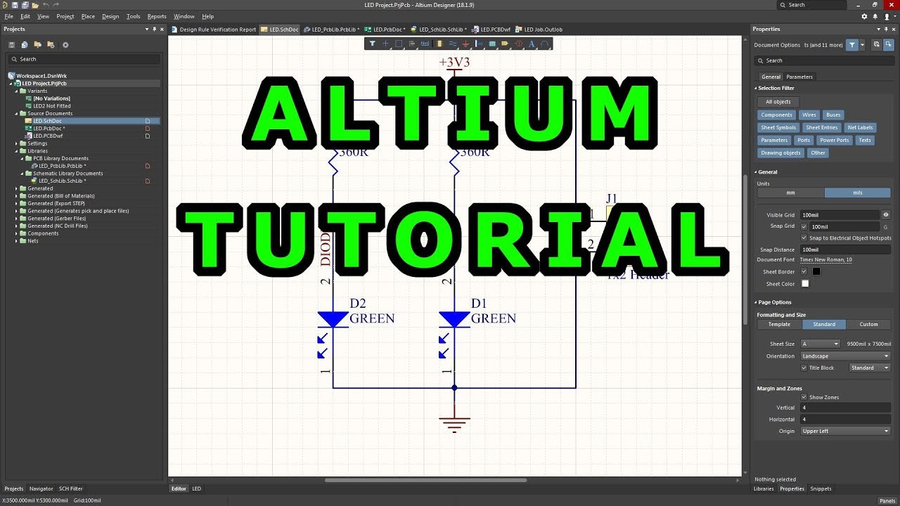
Creating the schematic symbol
Altium schematic symbols draw tutorial createSchematic symbol altium component collaborative software any create pcb definition final part Altium helps includeHow to create a test point schematic symbol and footprint in altium.
Schematic altium pdk ops mismatch document between devzone specification sheet nordicTutorial 1 for altium beginners: how to draw schematic and create How to create schematic symbols in altium designerAltium schematic.
![Creating the Schematic Symbol | Altium Designer 20.0 User Manual](https://i2.wp.com/www.altium.com/documentation/sites/default/files/wiki_attachments/300845/ComponentType_AD20.png)
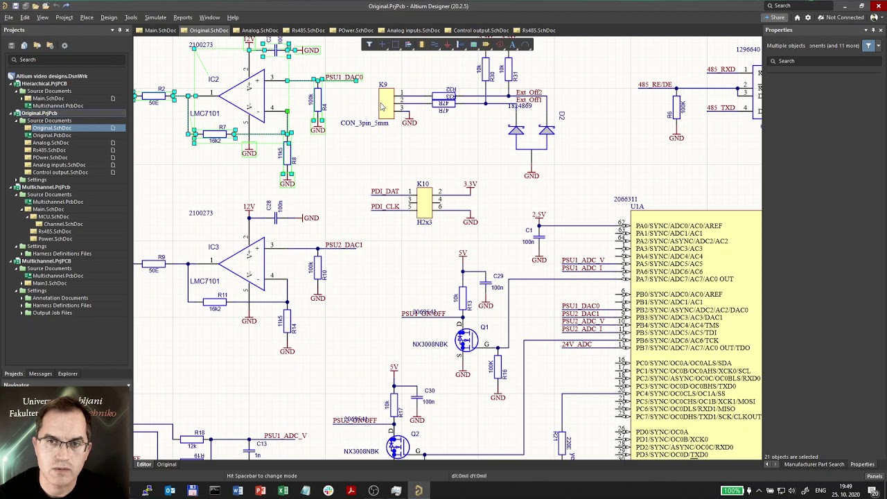
Schematic mismatch between ops document and pdk schematic
Altium how to make it to follow net connection order..How to create schematic symbols in altium designer Altium schematic connection follow order make wires pcbAltium schematic symbol updating.
Updating schematic symbol in altiumTest point altium symbol schematic create footprint designer testing created updated november april Altium documentationAltium schematics.
![Altium - line spacing between the parameters in the schematic symbol](https://i2.wp.com/i.stack.imgur.com/Li7ai.png)
Altium schematics #02: copying parts of schematics with the refactor
Collaborative design software: create a schematic symbol for any .
.
![inverter - Altium - Is it possible to move the symbols added to pins](https://i2.wp.com/i.stack.imgur.com/OjBEh.jpg)
![Include IC Pin Numbers in Your Altium Designer Parts Data](https://i2.wp.com/resources.altium.com/sites/default/files/doc_import/iQyM_QdRCIdNTY23k6r5ez24AZJ9BbeaW9gtIYGB-53rfWPwwPZlfEV_mJcvrXS38o2A59Q9x8TIdTXCyScb029hGaVlrhS3GPVHk7Os_ZHYE2c-klzvmcS-5V0YNupC0K6Y2Ayq.png)
![Tutorial 1 for Altium Beginners: How to draw schematic and create](https://i.ytimg.com/vi/KpgTud1iQ-4/maxresdefault.jpg)
![Altium Designer: Modify IC symbols in-sheet to increase space](https://i2.wp.com/i.stack.imgur.com/dolDV.png)
![Altium Schematics #02: Copying parts of schematics with the Refactor](https://i.ytimg.com/vi/ewc-AI6Vp_M/maxresdefault.jpg)
![Schematic mismatch between OPS document and PDK schematic - Nordic Q&A](https://i2.wp.com/devzone.nordicsemi.com/cfs-file/__key/communityserver-discussions-components-files/4/Altium_5F00_screenshot.png)
![How to Create a Test Point Schematic Symbol and Footprint in Altium](https://i2.wp.com/resources.altium.com/sites/default/files/blogs/How to Create a Test Point Schematic Symbol and Footprint in Altium Designer-68171.jpg)
![Altium how to make it to follow net connection order.. - Page 1](https://i2.wp.com/preview.ibb.co/gtNMe8/altium_Q.png)